H-Bridge Current Sensing
I intend to do some experiments with motor control and switching converters. Some of these experiments require to control currents in power electronic circuits, in particular the currents through inductive loads in H-bridge circuits. For that purpose, currents in H-bridges first have to be measured.
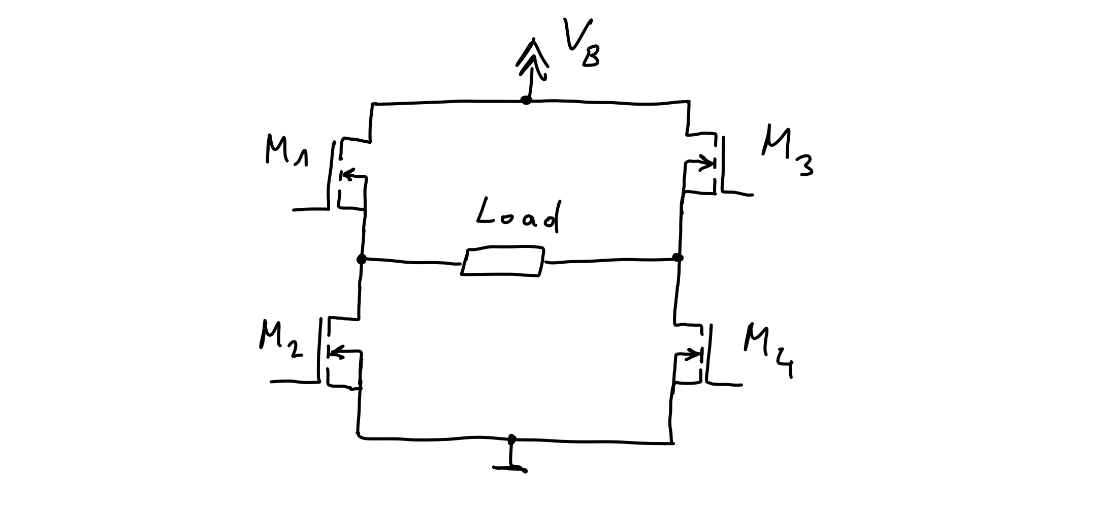
Consider a H-bridge as in Figure 1 below. Via PWM, an arbitrary voltage in the range \(-V_B,\ldots,V_B\) can be applied to the load. To apply a positive voltage to the load, M4 is permanently on and complementary PWM signals are applied to M1 and M2. In one PWM period of duration T, M1 is on for a certain time \(t_1\), then M1 is turned off and M2 is turned on for the remaining time \(t_2=T-t_1\), resulting in an average voltage of \(V_L=V_B\,t_1/T\) at the load. To apply a negative voltage to the load, M2 is permanently on and the PWM signals are applied to M3 and M4. (There are also other modulation schemes for controlling H-bridges, see e.g. this application report from TI, in which the design of output filters for Class-D audio amplifiers for different modulation schemes is discussed.) In motor control applications, the load presents some inductance. Depending on the PWM frequency and the inductance, the current through the load has some ripple. By choosing an appropriately high PWM frequency, this ripple can be reduced to a level which is acceptable for the application.
Current Sensing via Shunt Resistor
One way to measure a current is to measure the voltage drop over a shunt resistor caused by it, i.e. we simply have to connect a shunt resistor (typically several \(\mathrm{m}\Omega\) to several tens or a few hundred \(\mathrm{m}\Omega\)) in series with the load and measure the voltage drop over \(R_{shunt}\).
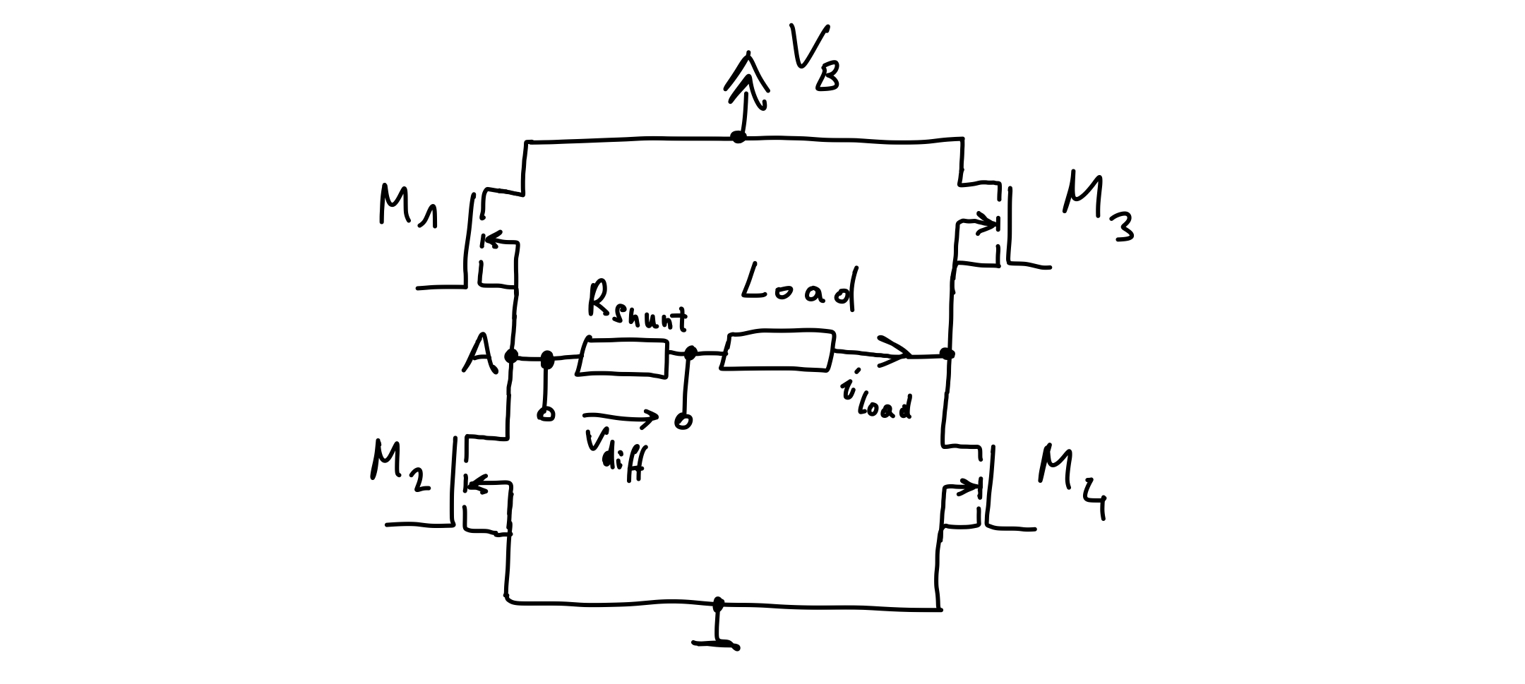
However, conditioning this voltage signal such that it can be measured with the AD-converter of a microcontroller is not a straight forward task. We are interested in the voltage drop \(V_{diff}\) across the shunt resistor. Therefore, a differential amplifier is needed. However, the differential amplifier must be able to handle a large common mode voltage. Due to the inductive nature of the load, the voltage at node \(A\) can even drop below the ground potential (by the voltage drop of the body diode of the MOSFET M2) and exceed the bus voltage \(V_B\) (by the forward voltage drop of the body diode of the MOSFET M1). (If we are dealing with a H-bridge or three half bridges as in three phase applications or some other configuration does not matter. In any case, measuring the current involves the conditioning of a small differential voltage under the presence of a large common mode voltage.) There exist highly specialized differential amplifiers designed specifically for current sensing applications in PWM controlled power electronic circuits which can handle this, e.g. the INA240, which can handle common mode voltages from \(-4\,\mathrm{V}\) to \(80\,\mathrm{V}\) while only supplied by \(5\,\mathrm{V}\) and which recovers from common mode transients within several hundred nanoseconds. However, this and comparable chips do not seem to be very common among hobbyists. I am not aware of commonly available breakout boards for this chip. The same applies to comparable current sense amplifiers like e.g. the MAX40056F
Other differential amplifiers which can handle very large common mode voltages are e.g. the INA149 or the AD628. Also these amplifiers seem to be well suited for current sensing applications, though their data sheets do not say a lot about their behavior under fast common mode transients as they occur in PWM controlled H-bridges. The INA149 has unity differential gain. In principle, the circuit used in this chip could be built with an operational amplifier and some precisely selected resistors. The principle circuit in the AD628 is not complicated either. It consists essentially of two basic operational amplifier circuits, namely an operational amplifier configured as differential amplifier (with differential gain less than one to allow for large common mode signals, we analyze that in detail below) and an operational amplifier configured as non-inverting amplifier (the gain of this stage can be set by two external resistors). The simplicity of the principle circuits of these amplifiers made me wonder whether I can build such amplifiers myself, using only some commonly available operational amplifiers and metal film resistors. Let us first consider the following circuit (inspired by the schematic given in the data sheet of the AD628).
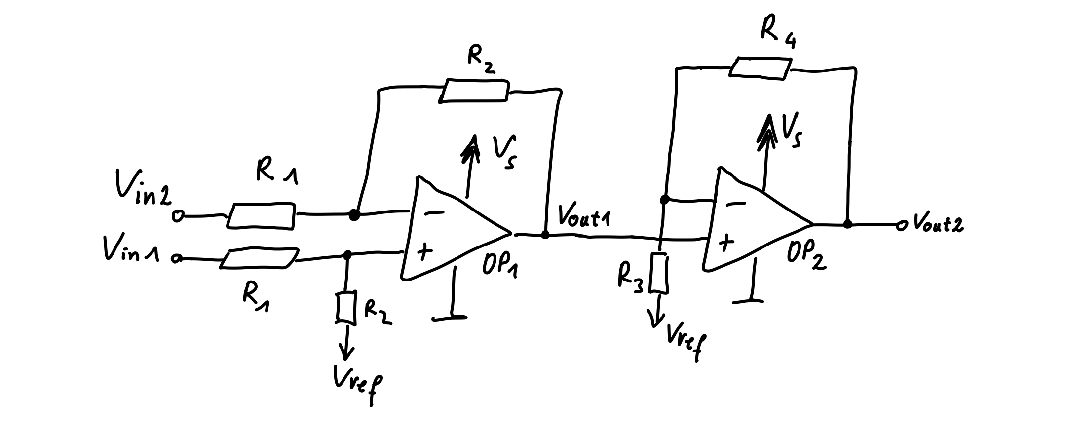
Let us analyze this circuit in regard to differential gain and the maximal admissible common mode voltage. The voltage at the inputs of \(OP_1\) must not exceed its supply voltage \(V_s\) and must not drop below the ground potential \(0\,V\). Opamps which can handle that are called rail-to-rail input amplifiers (similar to rail-to-rail output amplifiers, whose output voltage swing (almost) includes the supply rails). However, not all opamps are rail-to-rail input amplifiers, in which case an extra margin of typically several hundred \(\mathrm{mV}\) up to a few \(\mathrm{V}\) to the supply rails has to be taken into account. In the following, this margin is denoted \(V_m\).
Let \(V_{in1}=V_{cm}+1/2 V_{diff}\) and \(V_{in2}=V_{cm}-1/2 V_{diff}\), i.e. the voltage at the inputs of the circuit consists of a common mode component \(V_{cm}\) and a differential mode component \(V_{diff}\). Applying some basic network analysis methods, we find that the output voltage \(V_{out2}\) of this circuit is given by
\[\begin{align} V_{out2}&=V_{ref}+\tfrac{R_2}{R_1}(1+\tfrac{R_4}{R_3})V_{diff} \end{align}\]The common mode voltage \(V_{cm}\) has (ideally) no effect on the output voltage. The gain of the first stage, i.e. the ratio of \(R_2\) and \(R_1\) is limited by the admissible common mode voltage at the inputs of \(OP_1\). The voltage at the inputs of \(OP_1\) follows as
\[\begin{align} (V_{cm}+\tfrac{1}{2}V_{diff})\tfrac{R_2}{R_1+R_2}+V_{ref}\tfrac{R_1}{R_1+R_2} \end{align}\]and as discussed above, this voltage must not exceed \(V_S-V_M\) and must not drop below \(V_M\), i.e.
\[\begin{align} V_m\leq (V_{cm}+\tfrac{1}{2}V_{diff})\tfrac{R_2}{R_1+R_2}+V_{ref}\tfrac{R_1}{R_1+R_2}\leq V_s-V_m \end{align}\]In our application, the common mode voltage swings approximately between \(0\,\mathrm{V}\) and the bus voltage \(V_B\), whereas the differential mode voltage is only the voltage drop across the shunt resistor, i.e. we may neglect \(V_{diff}\) compared to \(V_{cm}\) for determining bounds on the ratio of \(R_2\) and \(R_1\). Furthermore, it is obviously reasonable to assume \(V_m<V_{ref}<V_s-V_m\). The first part of the inequality is relevant for negative \(V_{cm}=V_{cm,min}\) with \(V_{cm,min}<0\,\mathrm{V}\) (which can occur with inductive loads), and yields
\[\begin{align} R_2/R_1&\leq\tfrac{V_{ref}-V_m}{V_m-V_{cm,min}}&\text{(with}~V_{cm,min}<0\,\mathrm{V}\text{)} \end{align}\]The other part of the inequality is relevant for \(V_{cm}=V_{cm,max}\) and yields the restriction
\[\begin{align} R_2/R_1&\leq\tfrac{V_s-V_m-V_{ref}}{V_{cm,max}-V_s+V_m}&\text{(with}~V_{cm,max}>V_s-V_m\text{)} \end{align}\]Example 1:
For \(V_s=5\,\mathrm{V}\), \(V_{ref}=2.5\,\mathrm{V}\), \(V_{m}=0\,\mathrm{V}\) (rail-to-rail input amplifier) and \(V_{cm,min}=-1\,\mathrm{V}\) as well as \(V_{cm,max}=25\,\mathrm{V}\) (corresponding to a bus voltage of the H-bridge of \(V_B=24\,\mathrm{V}\)), an upper bound on the ratio of \(R_1\) and \(R_2\), and thus the gain of the first amplifier stage, is given by \(R_2/R_1\leq 2.5\) due to the first inequality and \(R_2/R_1\leq 0.125\) due to the second inequality. So in this example, the first stage actually dampens the signal by a factor of \(8\). Damping the signal in the first stage and amplifying it in the second stage makes the circuit susceptible for offset voltages of the opamps and noise.
Another problem of this circuit is its common mode gain. Ideally, i.e. with perfectly matched resistors, the common mode gain of the circuit is zero. However, in practice the resistors \(R_1\) and \(R_2\) connected to the inverting input of \(OP_1\) will slightly differ from \(R_1'\) and \(R_2'\) connected to the non-inverting input of \(OP_1\), see the figure below.
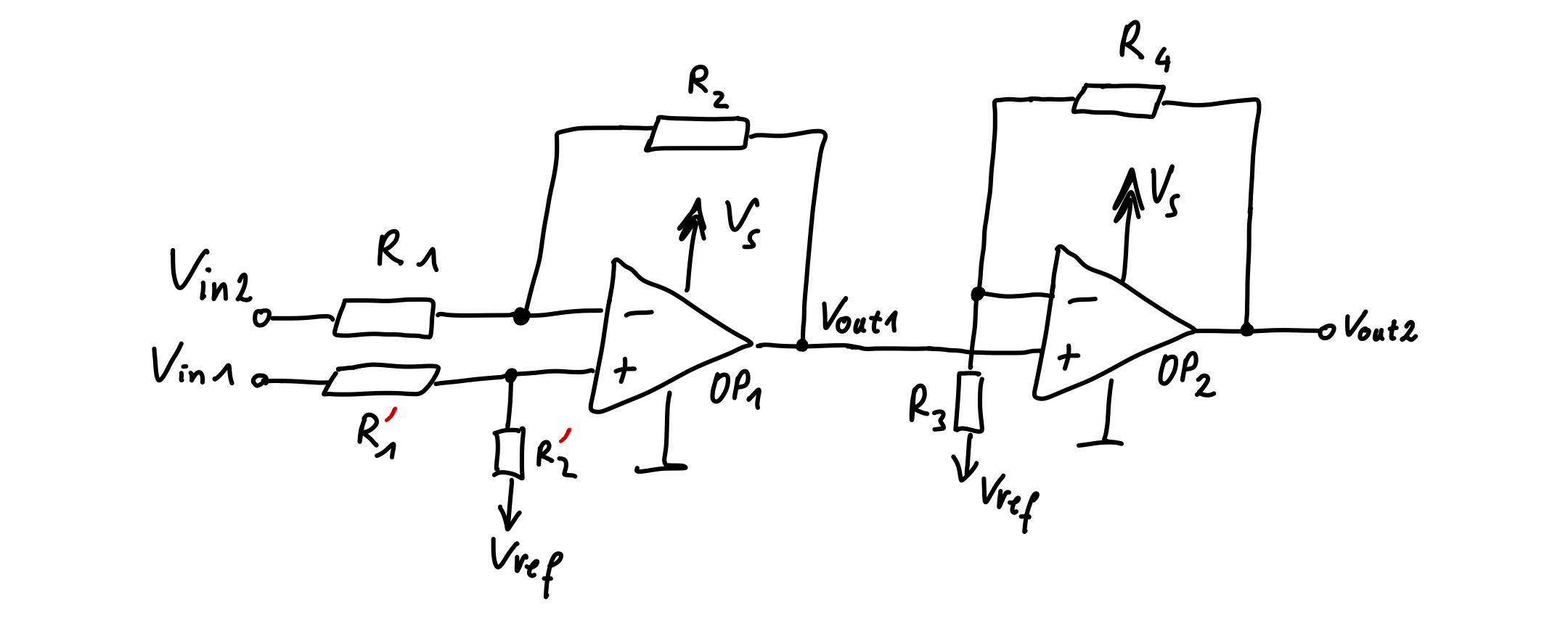
A mismatch of the ratios \(R_2/R_1\) and \(R_2'/R_1'\) causes a common mod gain. Let \(R_2'/R_1'=(1+\epsilon)R_2/R_1\), i.e. for \(\epsilon=0\) the resistor ratios are perfectly matched, the larger \(\epsilon\) the worse is the match. For the above circuit one derives
\[\begin{align} V_{out2}&=V_{ref}+\left[\tfrac{\epsilon}{1+\tfrac{R_2}{R_1}(1+\epsilon)}V_{cm}+\left(1+\tfrac{\epsilon}{2\left(1+\tfrac{R_2}{R_1}(1+\epsilon)\right)}\right)V_{diff}\right]\tfrac{R_2}{R_1}(1+\tfrac{R_4}{R_3})\\ &\approx V_{ref}+\left(\tfrac{\epsilon}{1+\tfrac{R_2}{R_1}}V_{cm}+V_{diff}\right)\tfrac{R_2}{R_1}(1+\tfrac{R_4}{R_3}) \end{align}\]The common mode rejection ratio, which is the ratio of the differential mode gain and the common mode gain (and is usually given in \(\mathrm{dB}\)) of this circuit is thus approximately
\[\begin{align} CMMR\approx\tfrac{1+\tfrac{R_2}{R_1}}{\epsilon} \end{align}\]A high \(CMMR\) is crucial in our application since the common mode voltage \(V_{cm}\) is in the range of the bus voltage \(V_B\), whereas the differential mode voltage \(V_{diff}\), i.e. the voltage drop across the shunt resistor, is only in the range of at most a few hundred \(\mathrm{mV}\).
Example 2:
With \(R_2/R_1=0.125\) (see Example 1) and \(0.1\%\) resistors, the worst-case mismatch of the resistor ratios is \(\epsilon=1.001^2/0.999^2-1\approx 0.004\), we achieve \(CMMR\approx 281\). A swing of the common mode voltage between \(0\,\mathrm{V}\) and \(24\,\mathrm{V}\) causes the same swing of the output voltage \(V_{out1}\) of the differential amplifier as a differential mode voltage swing of approximately \(0.085\,\mathrm{V}\). In conjunction with a shunt resistor of e.g. \(200\,\mathrm{m\Omega}\), this corresponds to an error in the measured current of \(425\,\mathrm{mA}\).
According to the above formula, a high \(CMMR\) is achieved by a good match of the resistors (i.e. a small \(\epsilon\)) and a large ratio \(R_2/R_1\). Above we have seen that \(R_2/R_1\) is limited by the admissible common mode voltage at the inputs of \(OP_1\).
Improving the CMMR
Above, we have derived that \(CMMR\approx (1+R_2/R_1)/\epsilon\), i.e. the \(CMMR\) improves with a larger resistor ratio \(R_2/R_1\). This resistor ratio is also the differential gain of the circuit, so a larger ratio is indeed desireable. However, as we have also seen above, the ratio \(R_2/R_1\) is limited by the common mode signal which the circuit has to be able to handle (see Example 1 above). Raising the supply voltage \(V_s\) of \(OP_1\) to the bus voltage \(V_B\) of the H-bridge (for low voltage applications, i.e. \(V_B=24\,\mathrm{V}\), this can easily be done with standard opamps) and choosing \(V_{ref}=V_s/2\) allows for the largest resistor ratio \(R_2/R_1\) (a 78xx fixed voltage regulator may be used for generating \(V_{ref}\) from (filtered) \(V_B\)). Recall that with an inductive load in the H-bridge, the common mode voltage can exceed \(V_B\) and drop below \(0\,\mathrm{V}\) by the voltage drop of the body diode of the corresponding MOSFET, i.e. about \(1\,\mathrm{V}\) (though this only occurs during the short period of dead-time in which none of the MOSFETs is turned on). Taking this transient into account, i.e. requiring that the circuit can handle a common mode voltage of \(-V_{Diode}\) to \(V_B+V_{Diode}\), and choosing \(V_s=V_B\) as well as \(V_{ref}=V_s/2\) yields (for a rail-to-rail input amplifier)
\[\begin{align} R_2/R_1&\leq\tfrac{V_B}{2V_{Diode}}\,. \end{align}\]Consequently, the ratio \(R_2/R_1\) and thus the \(CMMR\) can be improved significantly. The output of \(OP_1\) is now of course centered at \(V_{ref}=V_s/2\) and may swing between approximately \(0\,\mathrm{V}\) and \(V_s\). Therefore, in the circuit below, the voltage divider formed by \(R_3\) and \(R_4\) is used for conditioning the signal for ADC inputs. The overall differential gain is thus \(A_{Diff}=\tfrac{R_2}{R_1}\tfrac{R_4}{R_3+R_4}\). A drawback of the proposed circuit is that \(V_{ref}\) cannot be used directly in a differential input ADC, it also needs to be divided down by a voltage divider with resistor values \(R_3\) and \(R_4\). (When only using a single ended ADC, this additional voltage divider is of course not needed. However, then inaccuracies of \(V_{ref}\) directly influence the current reading.)
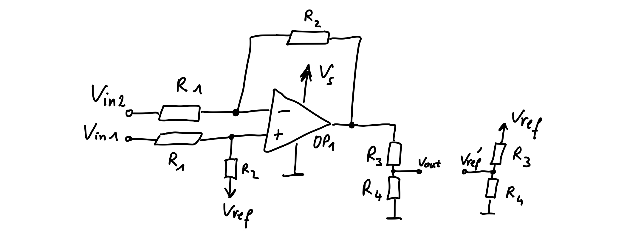
For the above circuit, one derives the following formula for the output voltage
\[\begin{align} V_{out}&=\underbrace{\tfrac{R_4}{R_3+R_4}V_{ref}}_{V_{ref}'}+\underbrace{\tfrac{R_2}{R_1}\tfrac{R_4}{R_3+R_4}}_{A_{diff}}V_{diff} \end{align}\]Taking into account a mismatch of the resistors, where \(R_2'/R_1'=(1+\epsilon_1)R_2/R_1\) and \(R_4'/R_3'=(1+\epsilon_2)R_4/R_3\) and an offset voltage \(V_{os}\) of the opamp, as illustrated in Figure 6 below
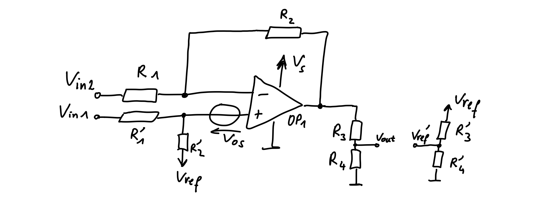
one derives
\[\begin{align} V_{out}&=\tfrac{R_4}{R_3+R_4}V_{ref}\left[\tfrac{\epsilon_1}{1+\tfrac{R_2}{R_1}(1+\epsilon_1)}V_{cm}+\left(1+\tfrac{\epsilon_1}{2\left(1+\tfrac{R_2}{R_1}(1+\epsilon_1)\right)}\right)V_{diff}\right]\tfrac{R_2}{R_1}\tfrac{R_4}{R_3+R_4}\\ &\hspace{2ex}+\left(1+\tfrac{R_2}{R_1}\right)\tfrac{R_4}{R_3+R_4}V_{os}\\ &\approx \tfrac{R_4}{R_3+R_4}V_{ref}+\left[\left(\tfrac{\epsilon_1}{1+\tfrac{R_2}{R_1}}V_{cm}+V_{diff}\right)\tfrac{R_2}{R_1}+\left(1+\tfrac{R_2}{R_1}\right)V_{os}\right]\tfrac{R_4}{R_3+R_4} \end{align}\]and for the difference \(V_{out}-V_{ref}'\), which is relevant when an ADC with differential inputs is used, we obtain
\[\begin{align} &V_{out}-V_{ref}'\approx\\ &\hspace{2ex}\left[-\epsilon_2\tfrac{R_3}{R_3+R_4}V_{ref}+\left(\tfrac{\epsilon_1}{1+\tfrac{R_2}{R_1}}V_{cm}+V_{diff}\right)\tfrac{R_2}{R_1}+\left(1+\tfrac{R_2}{R_1}\right)V_{os}\right]\tfrac{R_4}{R_3+R_4}\,. \end{align}\]Example 3:
Assume that we have \(V_s=V_B=24\,\mathrm{V}\) (the opamp may be supplied by a filtered version of the bus voltage, a varying bus voltage is not really a problem because the power supply rejection ratio of usual opamps is usually in the range of \(100\,\mathrm{dB}\)), a shunt resistor of e.g. \(200\,\mathrm{m\Omega}\) and a desired measuring range of \(\pm 2\,\mathrm{A}\), which should produce an output voltage \(V_{out}\) between \(1\,\mathrm{V}\) and \(4\,\mathrm{V}\) (i.e. centered at \(2.5\,\mathrm{V}\)). The required differential gain of the circuit is thus \(A_{Diff}=3.75\). The differential gain of the circuit is given by \(A_{Diff}=\tfrac{R_2}{R_1}\tfrac{R_4}{R_3+R_4}\). Since \(V_{out1}\) should be centered at \(2.5\,\mathrm{V}\) and \(V_{ref}=V_s/2=12\,\mathrm{V}\), it follows that \(R_4/(R_3+R_4)=5/24\) and consequently \(R_2/R_1=18\). Again with \(0.1\%\) resistors and the worst-case mismatch of the resistor ratios of \(\epsilon\approx 0.004\), we achieve \(CMMR\approx 4750\). A swing of the common mode voltage between \(0\,\mathrm{V}\) and \(24\,\mathrm{V}\) causes the same swing of the output voltage \(V_{out1}\) as a differential mode voltage swing of approximately \(0.005\,\mathrm{V}\). With the \(200\,\mathrm{m\Omega}\) shunt resistor, this corresponds to an error in the measured current of \(25\,\mathrm{mA}\), which is a significant improvement over the \(425\,\mathrm{mA}\) of the previous circuit. The larger the gain of the circuit, i.e. the larger the ratio \(R_2/R_1\), the larger is the effect of the offset voltage. In this example, a usual input offset voltage of \(OP_1\) of \(2\,\mathrm{mV}\) corresponds to an error of the measured current of approximately \(12.6\,\mathrm{mA}\).
Depending on the PWM frequency, the load inductance and its resistance, the current through the load has some ripple. To filter out this ripple, i.e. to sense the average current through the load, \(V_{out}\) has to be low pass filtered. Adding a capacitor with capacitance \(C\) in parallel to \(R_4\) results in low pass filtering with a cutoff frequency of \(f_c=\tfrac{R_3+R_4}{2\pi R_3R_4C}\).
Experimental Results
For testing the current sensing amplifier in practice, I have set up a test circuit on a breadboard. On the left, you can see a L6205 dual full bridge ic. It is wired up according to the typical application circuit provided in its data sheet (only one of the two full bridges is actually used). The shunt resistor is formed by two large \(1\,\Omega\) resistors in parallel (thus \(R_{shunt}=0.5\,\Omega\)), which you can see in the middle. (Such a setup is of course far from a proper Kelvin connection of the shunt resistor. The contact resistance of the breadboard, which depends on many factors and is thus not very well reproducible, adds to the shunt resistance. In my setup, with a brand-new breadboard, I measured a contact resistance below \(4\,\mathrm{m\Omega}\), which is negligible compared to the shunt resistance. However, for a lower value shunt resistor, I would solder sensing wires directly to its leads.) To the right, you can see a dual opamp, namely the very common LM358. One opamp in this package is the actual current sensing amplifier, set up according to Figure 4, the other one is used for providing the reference voltage of about half the supply voltage for the current sensing amplifier. The load is one winding of a stepper motor (approximately \(1\,\Omega\) and \(0.8\,\mathrm{mH}\)). The whole setup is supplied by roughly \(18\,\mathrm{V}\) from batteries (which drops to about \(15\,\mathrm{V}\) under load due to their internal resistance and the way to thin wire used for connecting them to the breadboard).
The actual current sensing amplifier is set up according to the circuit in Figure 5 using \(0.1\%\) resistors with nominal values \(R_1=10\,\mathrm{k\Omega}\), \(R_2=30\,\mathrm{k\Omega}\), \(R_3=30\,\mathrm{k\Omega}\), \(R_4=10\,\mathrm{k\Omega}\). Together with \(R_{shunt}=0.5\,\Omega\), this results in a sensitivity of \(0.375\,\mathrm{V/A}\). The PWM signal comes from a function generator. In one of the two half bridges, which together form the H-bridge, the low-side MOSFET is all the time on and the high-side MOSFET all the time off. The other half bridge is feed by the PWM signal. I tested \(10\,\mathrm{kHz}\) and \(50\,\mathrm{kHz}\) with \(20\%\) duty cycle in each case. The measurement results are presented below.
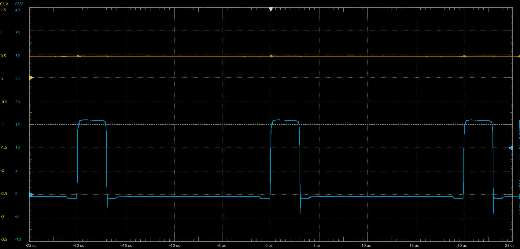
In Figure 8 below, you can see the measurement results for a PWM frequency of \(10\,\mathrm{kHz}\) with no load connected and no filtering (i.e. no capacitor in parallel to \(R_4\)). The top trace is \(V_{out}-V_{ref}'\) (which here should ideally be zero throughout) and the bottom trace is \(V_{in1}\) (i.e. the common mode input voltage of the current sense amplifier). Note that the vertical setting for both channels is different. The common mode gain of the amplifier is too low to be visible with the used vertical setting, however, the switching transients of the PWM are visible in the output signal.
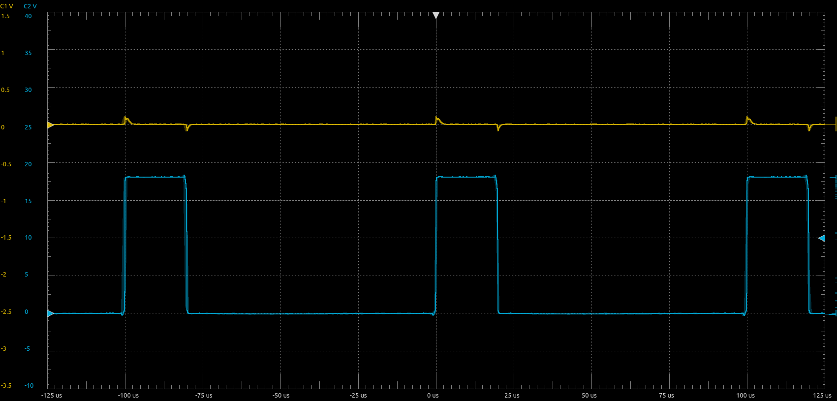
Figure 9 below shows the measurement results with the load connected. One can clearly see that the current through the load is rising during the on-time of the PWM and falling during the rest of the PWM period (during this time, the load is shorted via the two low-side MOSFETS of the H-bridge).
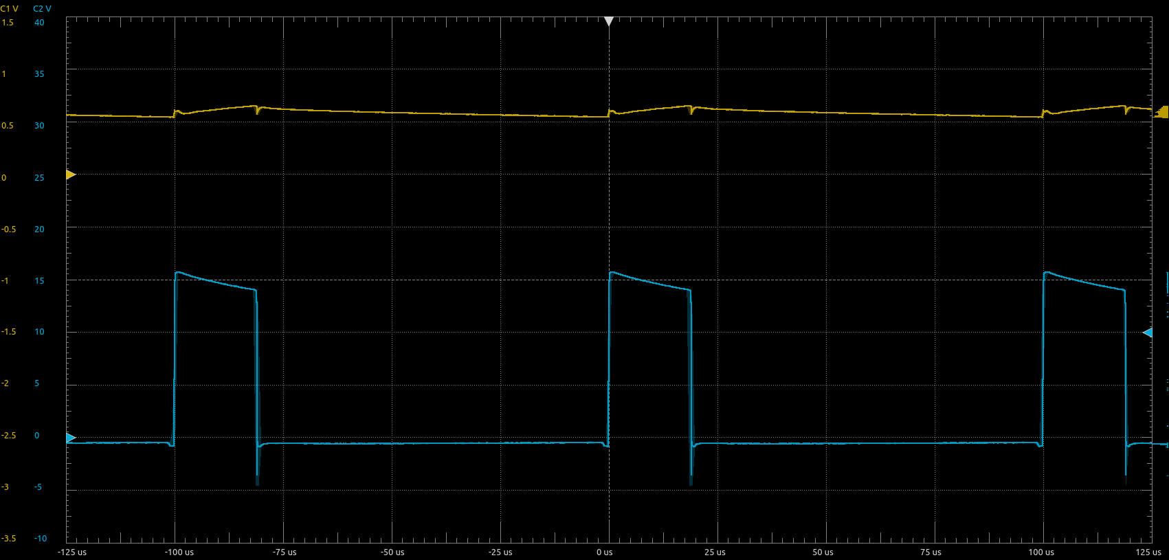
Figure 10 below shows the measurement results with the load connected and \(5\,\mathrm{nF}\) capacitance connected in parallel to \(R_4\). This results in a first order low pass filtering of the output signal with a cutoff frequency of approximately \(4.2\,\mathrm{kHz}\). The this way averaged output signal \(V_{out}-V_{ref}'\) is approximately \(0.55\,\mathrm{V}\), corresponding to an average load current of \(0.55\,\mathrm{V}/(0.375\,\mathrm{V/A})=1.47\,\mathrm{A}\). Measuring the voltage drop across the shunt resistor with a multimeter gave me a reading of \(0.720\,\mathrm{V}\), corresponding to an average current of \(0.72\,\mathrm{V}/R_{shunt}=1.44\,\mathrm{A}\). The relative error between these two measurements is thus only approximately \(2\%\).
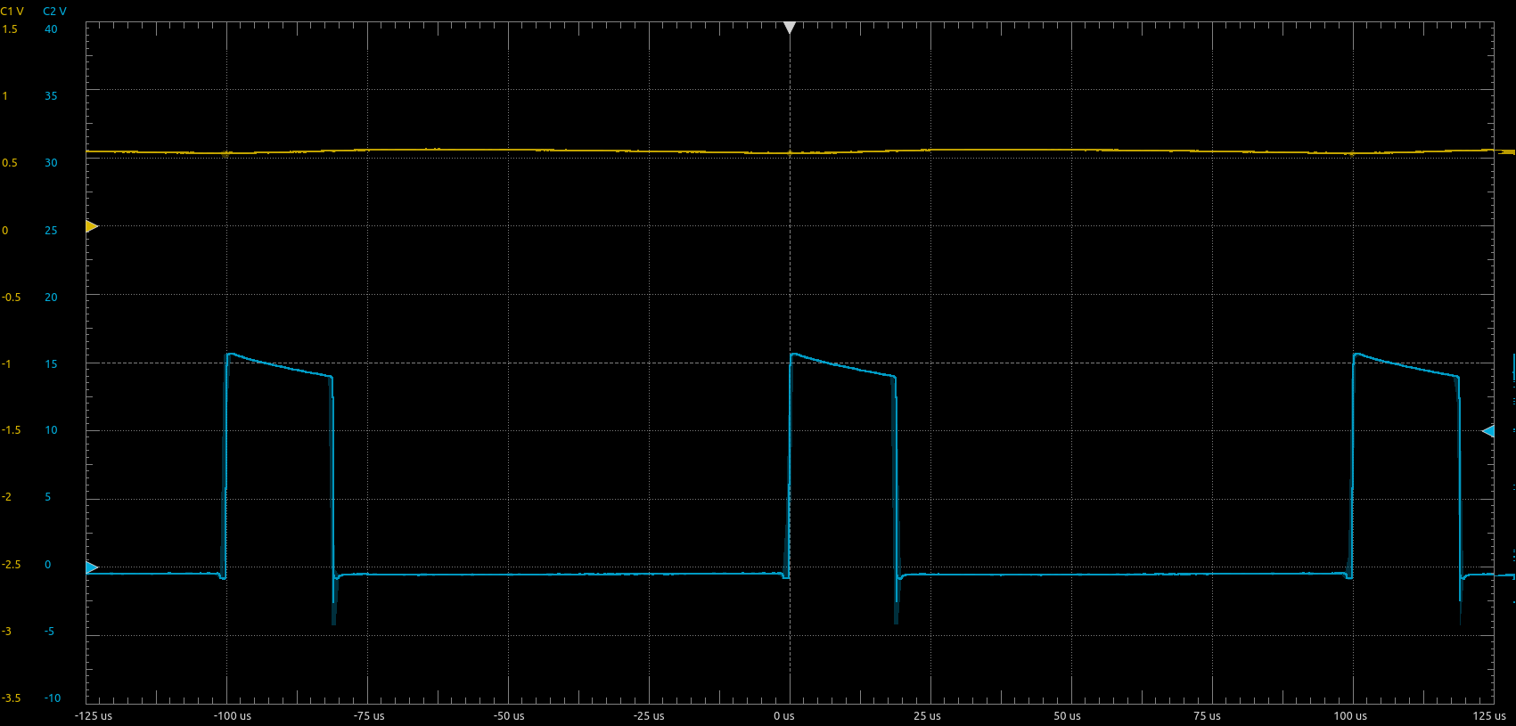
In Figure 11 below, the setup is exactly the same, except that the PWM frequency is \(50\,\mathrm{kHz}\). The averaged output signal \(V_{out}-V_{ref}'\) is approximately \(0.45\,\mathrm{V}\), corresponding to an average load current of \(0.45\,\mathrm{V}/(0.375\,\mathrm{V/A})=1.20\,\mathrm{A}\). Measuring the voltage drop across the shunt resistor with a multimeter gave me a reading of \(0.590\,\mathrm{V}\), corresponding to an average current of \(0.59\,\mathrm{V}/R_{shunt}=1.18\,\mathrm{A}\). (Although the duty cycle of the PWM signal generated by the function generator is in both cases \(20\%\), the actual duty cycle seen by the load is smaller when the frequency is higher due to the dead-time of the H-bridge, which is necessary to prevent cross conduction.)
Conclusion
Using a standard differential amplifier circuit based on an opamp seems to be feasible for current sensing in low voltage H-bridges with bus voltages of up to maybe \(30\,\mathrm{V}\). The accuracy depends on how well the used resistors are matched and the value of the shunt resistor. If a shunt resistor in the range of a few hundred \(\mathrm{m\Omega}\) is acceptable, reasonable accuracy can easily be achieved. However, such a self built current sensing amplifier may not be well suited for shunt resistances of only a few \(\mathrm{m\Omega}\). In general, I do not think that it is worth taking the hassle to build current sensing amplifiers yourself. In future projects, I will rather use current sensing amplifiers like the INA240, or use Hall effect (or flux gate) based current sensors like the LTS x-NP, CASR x-NP or T60404.
Hall Effect Current Sensing
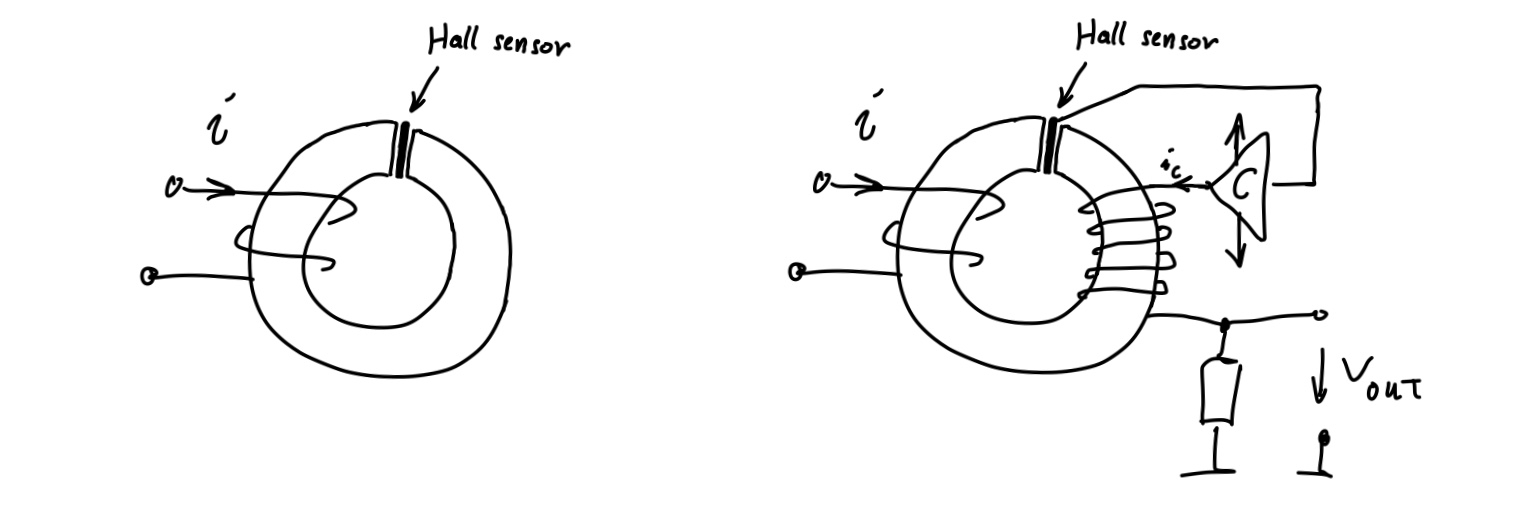
Besides measuring currents via the voltage drop over a shunt resistor, currents can also be measured via the magnetic fields caused by them. Magnetic fields can in turn be measured via the Hall effect. There are many current sensors available which rely on the Hall effect, for example the ACS712. This and similar current sensors provide a galvanic isolation between the current sensing path and the actual sensing circuit, which makes them perfectly suited for current sensing in H-bridges and other power electronic circuits. The ACS712 comes in an 8-Lead SOIC package, i.e. the same SMD package used e.g. for opamps. The current to be measured flows via a low resistance trace through the ic. In close proximity to this trace, a Hall sensor is placed. The amplified and conditioned output voltage of the Hall sensor is then proportional to the current flowing through the ic. The ACS712 is quite popular in the hobby electronics community, ready to use breakout boards for this chip are widely available. A drawback of this an similar current sensors is however that they are susceptible to external magnetic fields and the output signal is quite noisy (see data sheet for noise specifications). Other Hall effect based current sensors use a ferrite or iron powder core. The current to be measured flows through a loop of wire around the core and a Hall sensor is placed in an air gap of the core. Instead of these open loop sensors, which output the amplified voltage from the Hall sensor, there are also closed loop current sensors available. As with the open loop sensors, the current to be measured flows through a loop of wire around the core and a Hall sensor is placed in an air gap of the core, but an additional winding around the core is used for compensating the magnetic flux caused by the current to be measured. This is achieved by a feedback control loop, which controls the current through this compensation winding. The current needed for compensating the flux is related to the current in the primary winding via the turns ratio of the primary winding and the compensation winding. A current sensor based on this principle is e.g. the LTS 6-NP.