
Plasma Speaker Based on TL494
A “normal” speaker produces sound by vibrating a membrane. A plasma speaker on the other hand uses a high voltage arc for producing sound. In a nutshell, modulating the intensity of the arc with an audio signal, modulates the heating and thus expansion of the surrounding air, which creates the sound.
The design described in this article uses a flyback transformer for producing the high voltage arc. The intensity of the arc is varied via pulse with modulation (PWM).
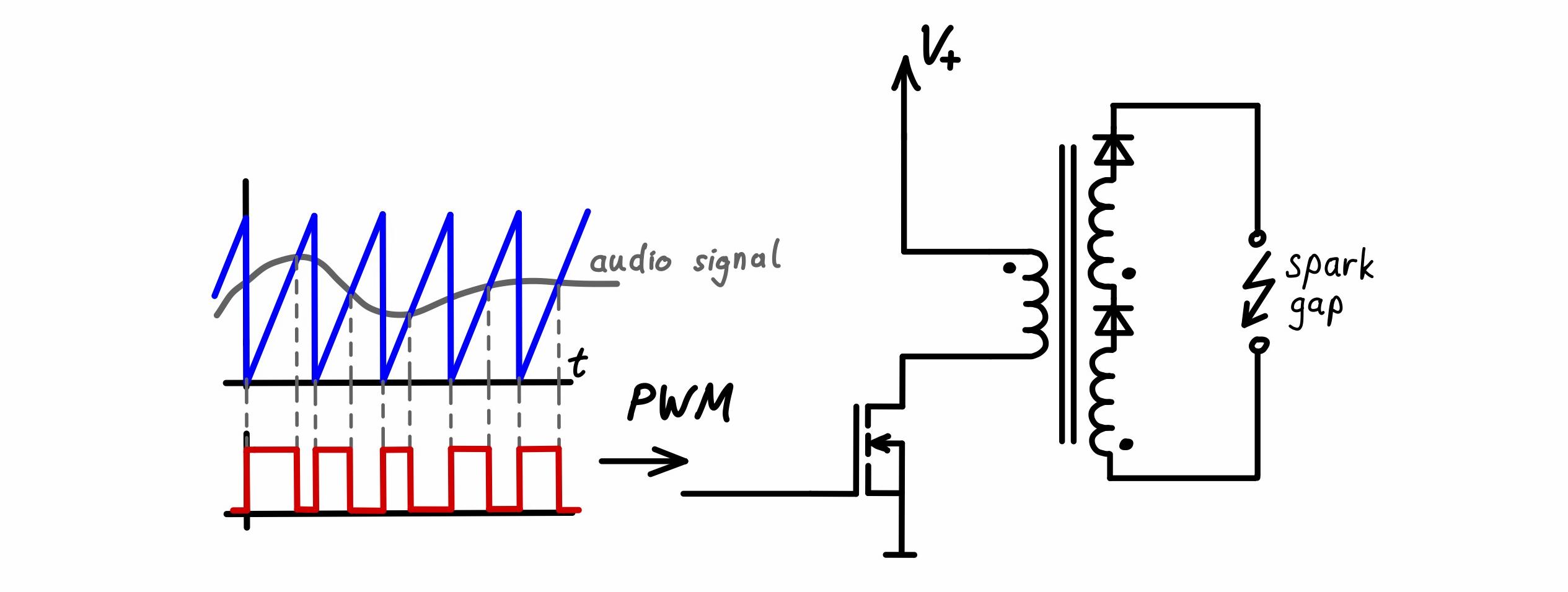
The flyback transformer in such a plasma speaker setup is indeed driven like the flyback transformer in a standard flyback converter circuit. During the ON-time of the PWM cycle, \(V_{supply}\) is applied to the primary of the flyback transformer. During this phase, the primary current and thus the magnetic flux in the core increase. Then, the MOSFET is turned off and the primary current rapidly drops to zero (a snubber may be used to protect the MOSFET from voltage spikes due to stray inductance), whereas the secondary current rapidly rises to approximately \(N_1I_1/N_2\) (\(N_1\) and \(N_2\) being the number of primary, resp. secondary turns and \(I_1\) the primary current at the instance of switching the MOSFET off). During the OFF-time of the PWM cycle, the magnetic flux in the core and the secondary current decrease. Then, the MOSFET is turned on again and the cycle repeats. During the ON-time, energy is stored in the transformer core (actually mostly in the air gap of the core). During the OFF-time, this energy is dumped into the plasma arc. The higher the duty ratio, the more energy is stored and then dumped into the arc. Therefore, modulating the duty ratio with an audio signal modulates the intensity of the arc. The duty ratio must not get too high, otherwise, the core may saturate. The circuit which I came up with can be seen in the figure below.
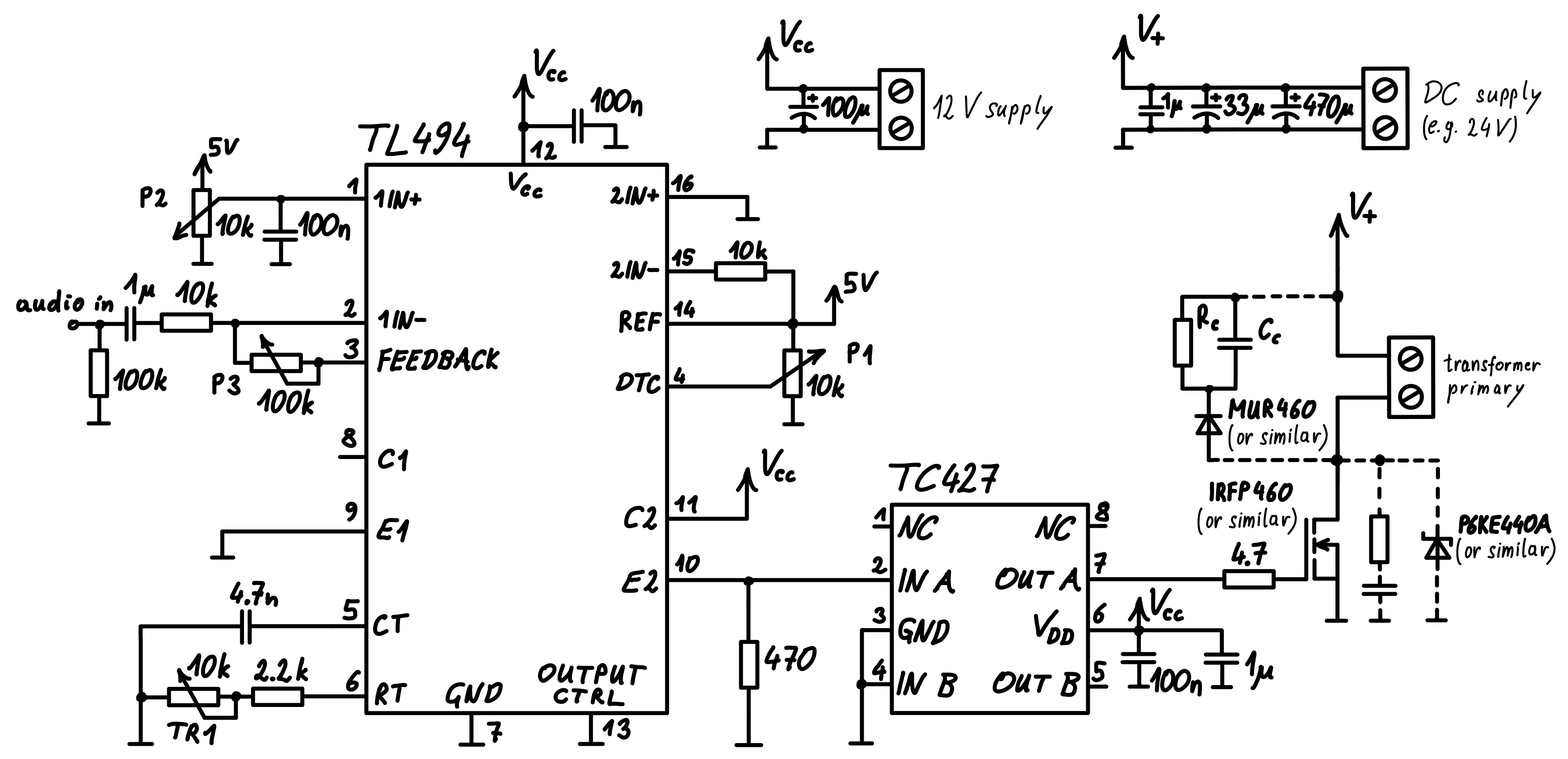
Similar circuits can be found e.g. on the sites https://scopeboy.com, https://paulside.com or https://www.instructables.com. Alternatives to the IRFP460 MOSFET would be e.g. IRFP450, IRFP440, IRF840, IRF740. Many application notes are available online which address the design of RCD clamps for flyback converters. As a rule of thumb, smaller values for \(R_c\) limit the voltage across the MOSFET to smaller values. However, choosing \(R_c\) too low results in poor performance, i.e., smaller output voltage. The value of \(C_c\) should be chosen large enough in order to limit the ripple of the voltage across this capacitor to acceptable values. The capacitor must be able to handle a few hundred volts and the resistor should be rated for a few watts. Instead of or additionally to the RCD clamp, an appropriate TVS diode (e.g. P6KE440A) or an RC snubber directly across the MOSFET may be used for protecting the MOSFET from voltage spikes.
In order to explain the working principle of the proposed circuit, let us have a look at the functional block diagram of the TL494, taken from its data sheet.
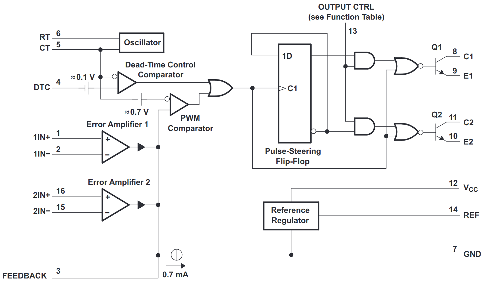
The internal oscillator generates a saw tooth signal (\(0\,\mathrm{V}\) to \(3.3\,\mathrm{V}\)). Its frequency can be adjusted between roughly \(20\,\mathrm{kHz}\) and \(100\,\mathrm{kHz}\) with the trimmer TR1 in Figure 2. This saw tooth signal is compared with the voltage at DTC and FEEDBACK for generating a PWM signal. The outputs of the comparators are ORed together. In the proposed circuit, the potentiometer P1 connected to the DTC input is used to limit the maximal duty cycle to a safe level (when DTC is connected to GND, the maximum duty cycle is approximately \(97\%\)). The signal present at the FEEDBACK pin is the audio signal amplified and with an offset. For amplifying the audio signal and adding an offset to it, Error Amplifier 1 is used. The amplification can be set via potentiometer P3 between \(0\) and \(10\). Via potentiometer P2, the idle voltage present at the FEEDBACK pin (and thus the idle duty cycle) is set. The other error amplifier is “deactivated” by connecting its non-inverting input to GND and pulling its inverting input high via a \(10\,\mathrm{k\Omega}\) resistor.
Practical Setup
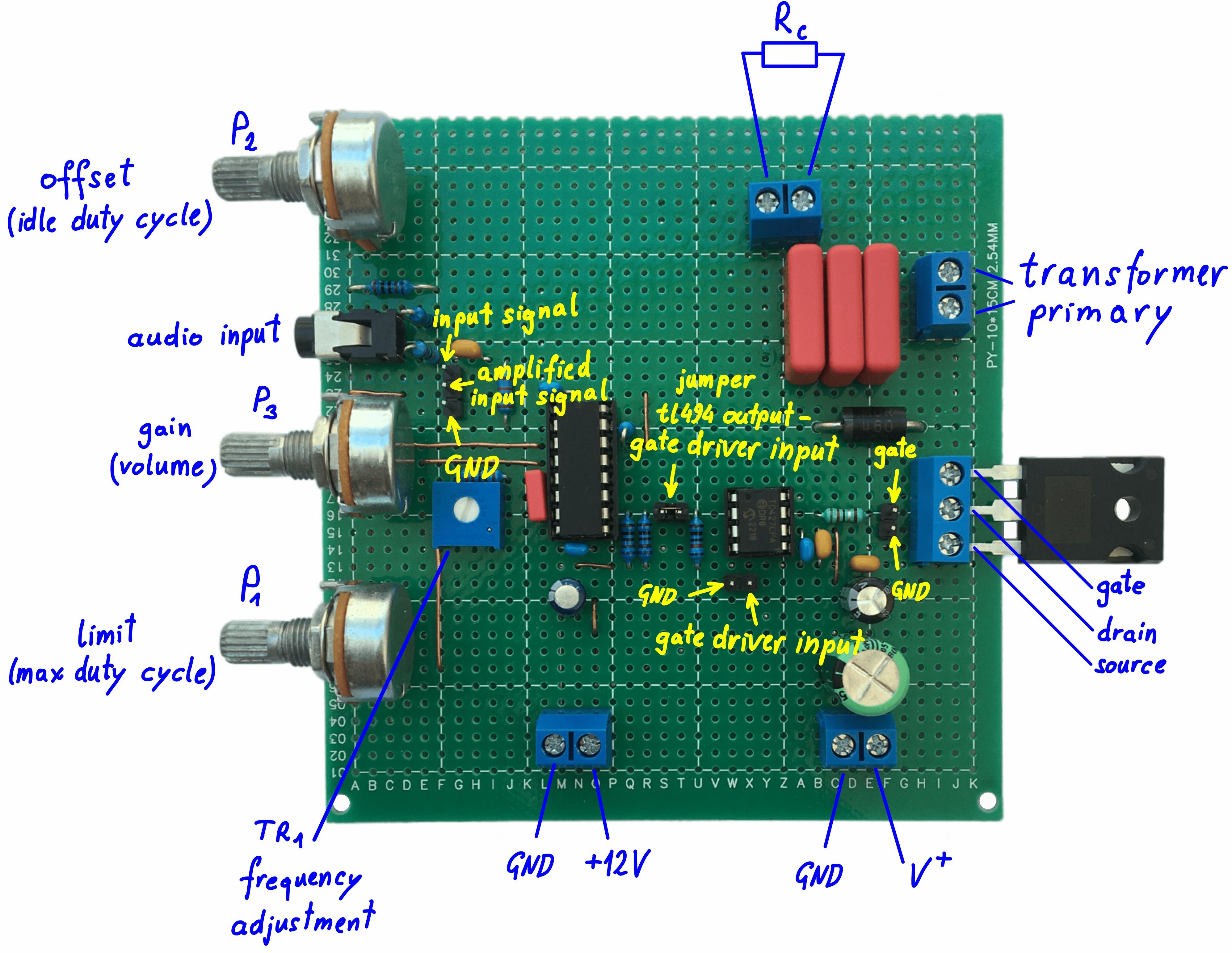
A practical realization of the driver circuit in Figure 2 can be seen in Figure 4 below. Instead of soldering the MOSFET directly to the board, I used screw terminals, which allows for quick and easy replacement of the MOSFET whenever necessary. For flexibility regarding the transformer characteristics, also the resistor of the RCD clamp is mounted via screw terminals and not soldered directly to the board. An additional RC snubber directly across the MOSFET or a TVS diode are not soldered to the board. I added a few pin headers as test points along the signal path (audio input signal, amplified audio signal at the FEEDBACK pin, input of the TC427, gate signal of the MOSFET). Additionally, I added a jumper between the output of the TL494 and the input of the TC427 (to whose input I soldered an additional \(10\,\mathrm{k\Omega}\) pull-down resistor to prevent an undefined state when the jumper is removed). The left- and the right channel of the stereo audio input are each connected to the “audio in” node in the above schematic via a \(1\,\mathrm{k\Omega}\) resistor, which combines the two channels to one mono channel.
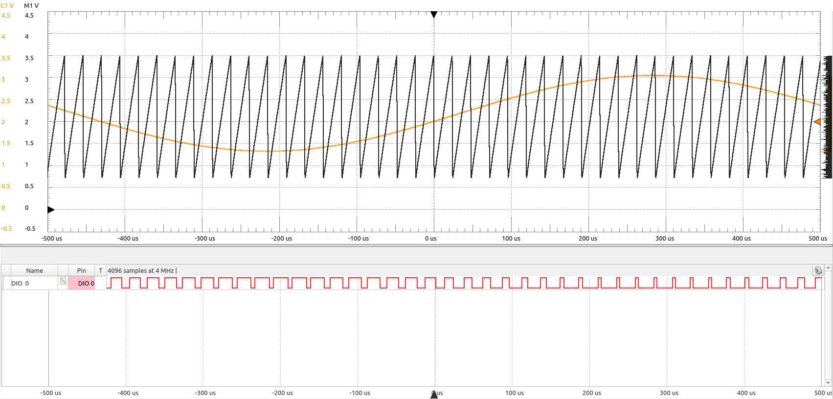
The oscilloscope measurements below illustrate the principle of operation. For taking these measurements, I supplied the driver and the power stage from the same \(12\,\mathrm{V}\) supply, i.e., the \(V_{CC}\) and \(V_{+}\) inputs were connected together and no transformer was connected. Scope channel C1 is the signal measured at the FEEDBACK pin of the TL494 (i.e., the amplified audio signal, in this case a \(1\,\mathrm{kHz}\) sine wave). Channel M1 is the saw tooth signal measured at pin 5 plus an offset of \(0.7\,\mathrm{V}\). This signal represents the signal at the inverting input of the PWM comparator, which is compared with the signal at the FEEDBACK pin (see block diagram in Figure 3). The digital channel DIO 0 shows the PWM signal at the gate of the IRFP460 power MOSFET (the used scope has only two analog channels, thus, one of its logic analyzer channels has been used for simultaneously capturing the three signals of interest). It can clearly be seen that the duty cycle of this PWM signal is modulated by the sine wave.
Regarding flyback transformers, I first used one which I salvaged from an old CRT TV. It was actually a so-called diode split flyback transformer, i.e., its secondary winding actually consists of several sections connected in series with high voltage diodes.
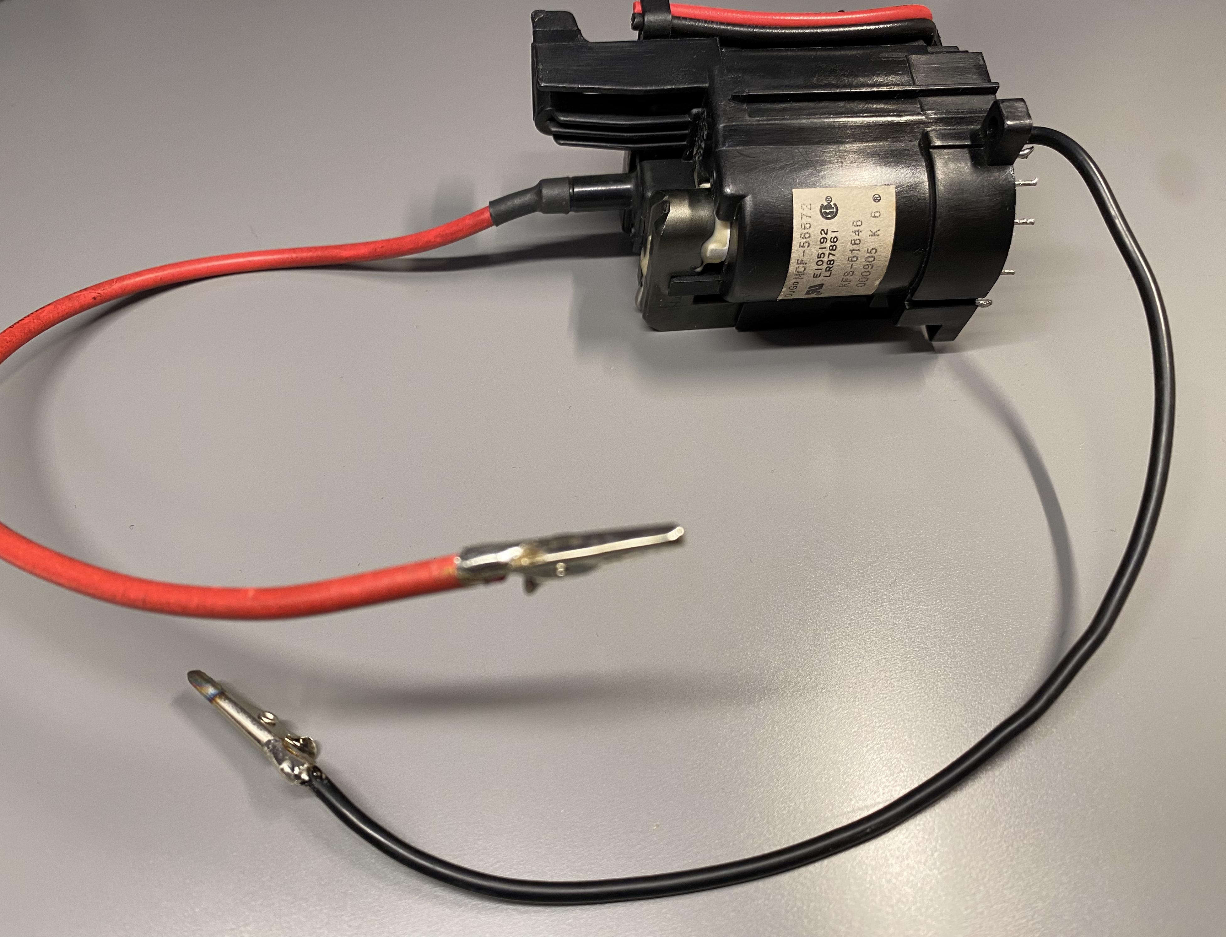
However, it got damaged after a few test runs due to an internal arcing between its windings, so later, I switched to an AC flyback transformer, i.e., a flyback transformer without diodes incorporated into its secondary winding, which I got from https://highvoltageshop.com/.
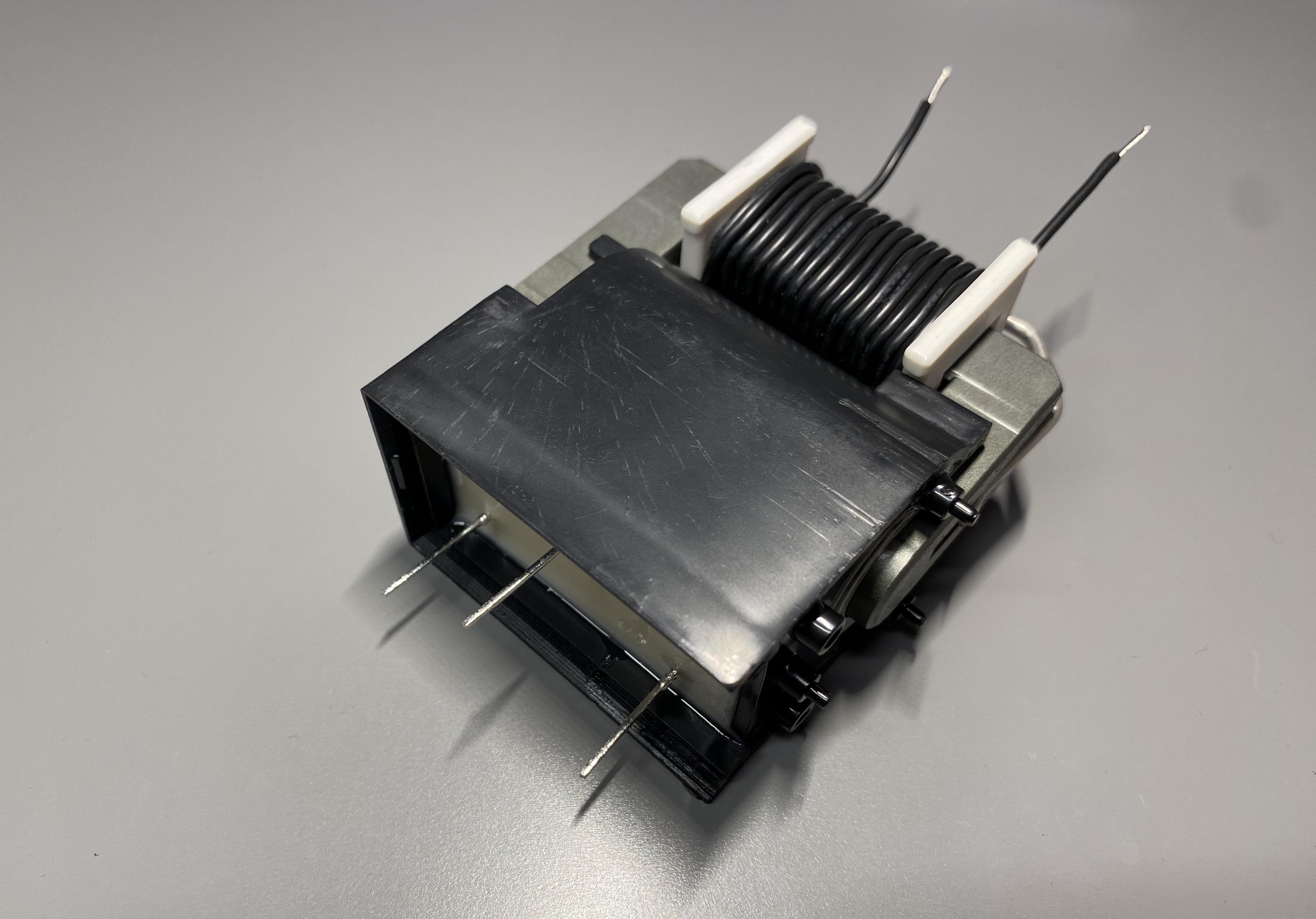
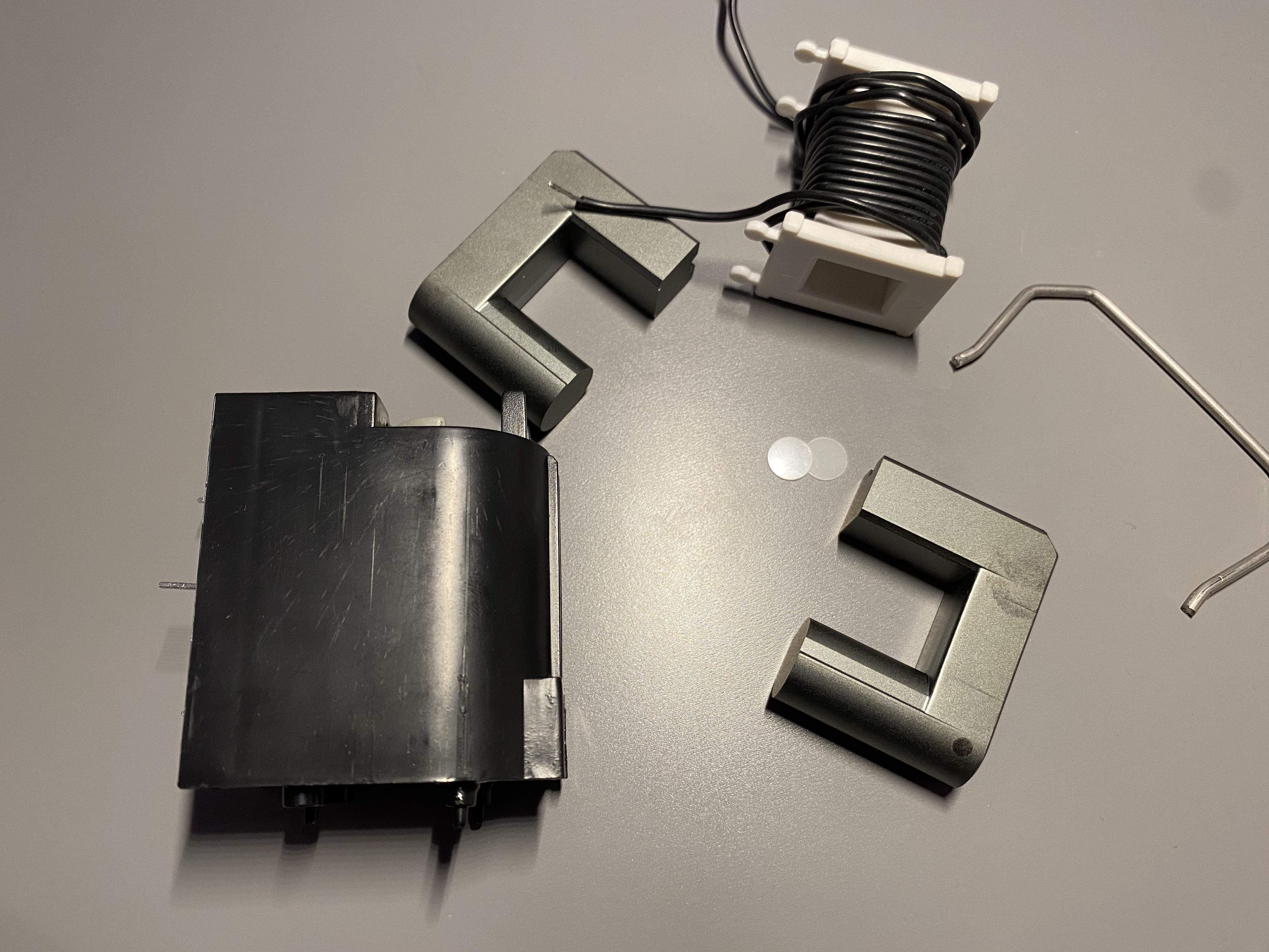
The ferrite core of this transformer, like the core of the diode split transformer in Figure 6, has an air gap, which significantly increases the current at which the core saturates and is crucial for proper operation of the plasma speaker. (The air gap is realized by placing to small plastic discs between the halfes of the ferrite core, see Figure 8.)
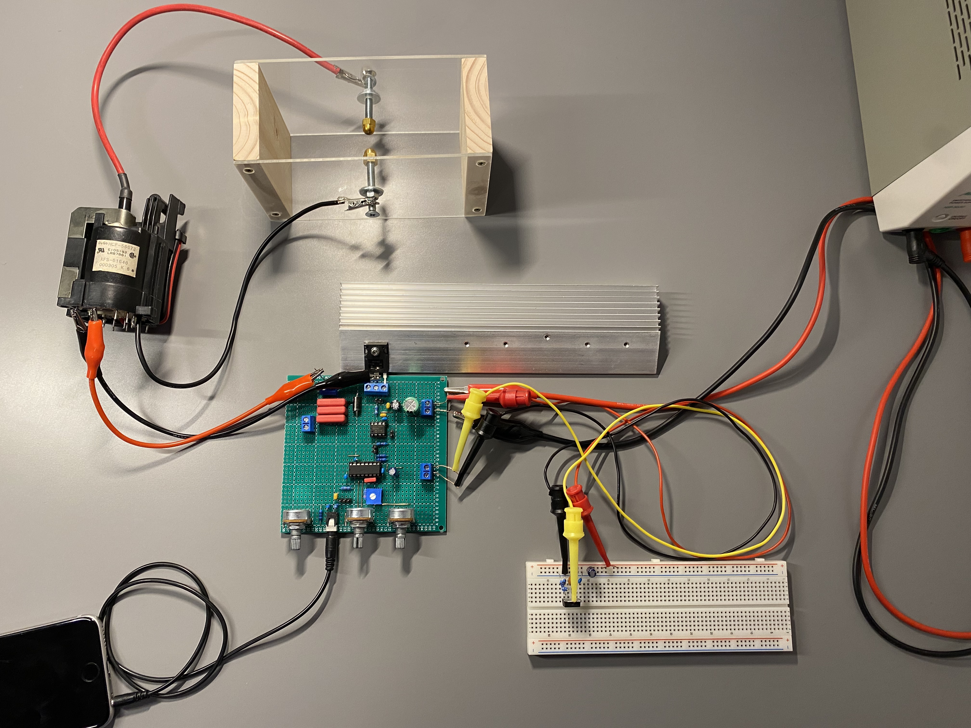
The complete test setup (with the diode split flyback transformer from Figure 6), can be seen in the figure below. In favor of performance, I ended up using no protection measures for the MOSFET. The RCD clamp is bypassed by disconnecting the drain of the MOSFET from the screw terminal and connecting one end of the transformer’s primary winding directly to the MOSFET’s drain. (To my surprise, the MOSFET handled this situation just fine, whereas the transformer got damaged after a while.) The power stage is supplied with \(24\,\mathrm{V}\) by a lab bench power supply. The driver stage is supplied by approximately \(12\,\mathrm{V}\), via the small breadboard circuit, using an LM317 voltage regulator. The PWM frequency is set to about \(40\,\mathrm{kHz}\). The spark gape is built from some wood, acrylic glass, screws, nuts and washers, and two brass cap nuts.
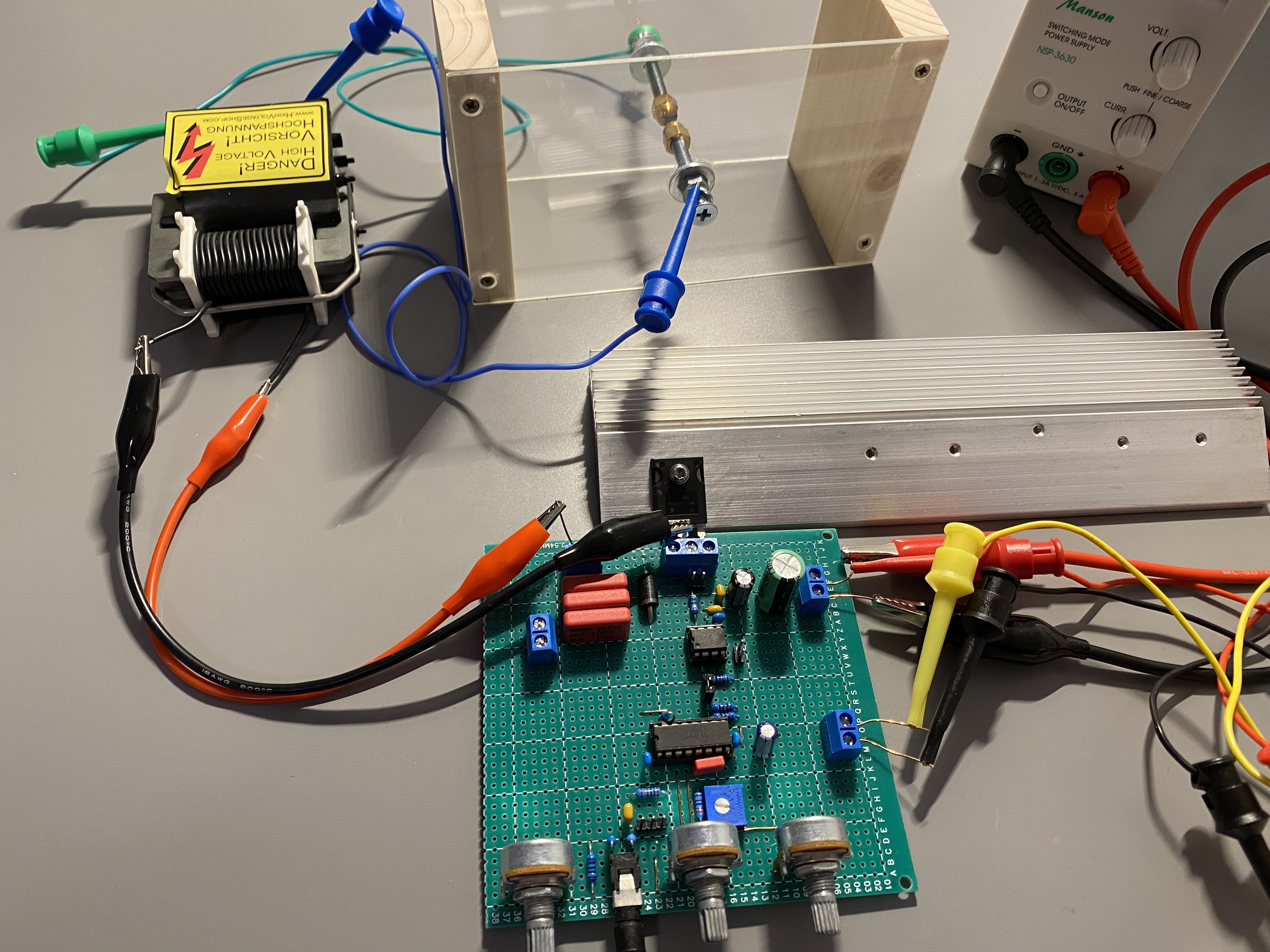
In Figure 10 below is the setup with the diode split flyback transformer replaced by the AC flyback from Figure 7. Compared to Figure 9, the length of the sparc gap has been reduced to only about \(4\,\mathrm{mm}\), in order to reduce the stress on the transformer’s internal insulation.
The video below shows a test run. In the beginning the idle duty cycle is zero. I slowly increase it by turing potentiometer P2 until some current is drawn from the power supply. The voltage at the spark gap does not suffice to ignite the arc, so I use a screw driver for igniting it. Once ignited, the arc is sustained. So fare, the arc is not modulated and is therefore almost completely silent. Next, I turn up the volume potentiometer P2 in order to modulated the arc with some music (the song is “Happy Morning” by Anton Kramar). Then, I turn the volume all the way up, which results in loud but extremely distorted audio. The volume is then turned back down to a reasonable level. Finally, the volume is turned all the way down (no modulation) and then also the idle duty cycle is turned down to zero.
Conclusion
The proposed plasma speaker setup achieves decent sound quality and producing sound this way is indeed very fascinating. It is of course needless to say that producing sound via a plasma arc is absolutely impractical. Besides hilariously poor efficiency, the arc radiates UV light and generates ozone and nitrogen oxides. I do not recommend rebuilding this plasma speaker. High voltage can be dangerous.